Integrate Meta Optical Components into Optical Systems Seamlessly
System Design
The importance of System Integration
System integration is important for optical design because it allows for the seamless integration of various optical components and subsystems into a complete and functional optical system.
Optical design involves the selection and optimization of individual optical elements such as lenses, mirrors, filters, and detectors. However, the performance of an optical system is not solely determined by the individual components but also by how these components work together.
Overall, system integration in optical design ensures that the individual optical components work together effectively, resulting in optimized performance, compatibility, and functionality of the complete optical system.
With the dawn of Meta Optics there is the need to do excellent system integration for Meta Optics and Meta Surfaces. System Design rules all and Meta Optics is no exception to this rule.
Key reasons why System Integration is crucial
Performance optimization: Integrating optical components into a system allows for the optimization of their collective performance. By considering the system as a whole, designers can take into account factors like alignment tolerances, stray light management, and overall system efficiency. This ensures that the optical system meets the desired performance specifications and achieves the desired functionality.
Compatibility and alignment: Integrating different optical components often requires precise alignment and compatibility considerations. Components such as lenses, detectors, and filters need to be aligned correctly relative to each other to achieve proper optical performance. Integration facilitates the alignment process and ensures that all components work together seamlessly.
System-level considerations: Optical systems are often part of larger systems, such as imaging systems, spectroscopy setups, or communication systems. Integration enables optical designers to consider system-level requirements and constraints, such as mechanical interfaces, thermal management, electrical connections, and packaging considerations. This holistic approach ensures that the optical system can be easily integrated into the larger system and meets all the necessary functional requirements.
Cost and time efficiency: Integrating optical components into a system can lead to cost and time savings. By considering system-level constraints and requirements early in the design process, designers can avoid costly iterations and modifications at later stages. Additionally, integrated optical systems can be manufactured and tested more efficiently since the interfaces and interactions between components are carefully planned and optimized.
Reliability and manufacturability: System integration allows for the consideration of reliability and manufacturability aspects. Designers can analyze and address potential failure points, thermal effects, material properties, and manufacturability challenges during the integration process. This leads to more robust and reliable optical systems that can be manufactured with higher yield and lower costs. Find more out the fabrication of Meta Optics via this link and via this link ( links to PDK website PlanOpSim + articles about Meta Optics Fabrication ).
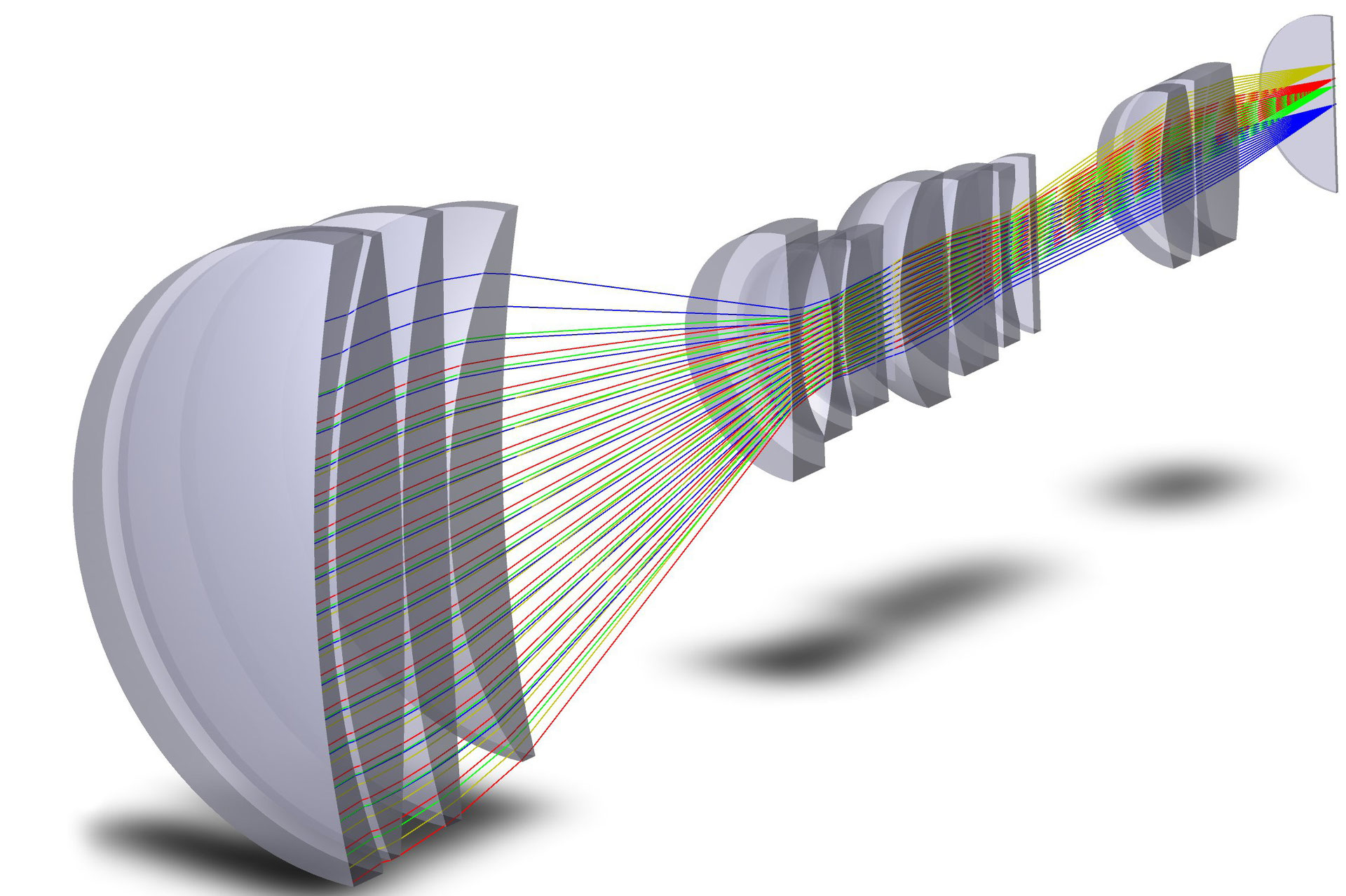
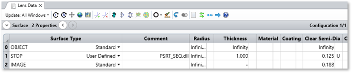
PlanOpSim specialises in the detailed calculations for meta-atoms and meta-component layout rather than ray tracing calculations. However, a ray tracing capability is necessary to integrate a meta-surface into a full optical system. For example, one ray tracing package is Zemax OpticStudio®.
The process of integrating the PlanOpSim calculations with Zemax OpticStudio® is quite straightforward and is split into two major components. The first is using PlanOpSim to design the meta surface and generate the desired near field wavefront target in PlanOpSim. The second step is to export these calculations as a PSRT file and import them into a Zemax OpticStudio® with the provided DLL plugin. Now the PSRT and DLL can used by Zemax OpticStudio®(*) for system level designing.
Below you will also find a video to see how it works in practice. ” Ray Tracing Link – Detailed Video ”
(*) Only valid for the legacy version of Zemax OpticStudio®.
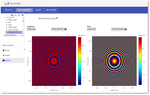
Example wavefront simulation of a metasurface
Step 1: Meta-lens design
The starting point is to design a meta-surface in the meta-component module. The wavefront or wavefronts can be derived from analytical design or optimizations in ray tracing software.
The end result is a meta-surface that approximates the intended target wavefront.
The wavefront can be simulated for various angles of incidence, wavelengths and polarization.
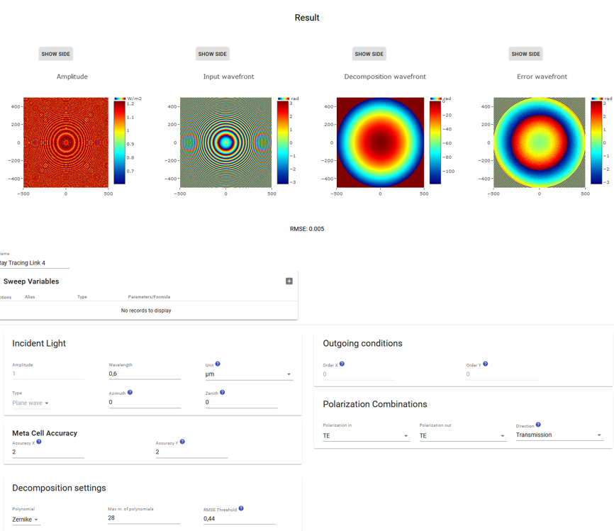
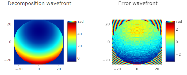
Step 2: Decompose the wavefront
In this step a phenomenological description of the meta-surface is made to be used in a system simulation in ray-tracing. This is done via the “psrt” file.
The PlanOpSim software decomposes the discrete wavefront which includes phase and amplitude errors into smooth functions. The wavefront of a meta-surface can differ strongly for different incident conditions. For example in a wavelength multiplexed design an independent lens shape is set for different wavelengths. The psrt file carries information for each incident light setting of interest for the system. In this way the specific angle, polarization and wavelength dependence can be captured.
After decomposition the psrt file and dll file are downloaded for import into ray-tracing.
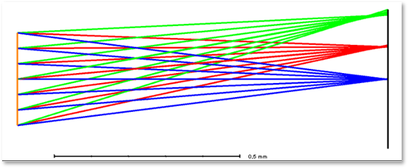
Step 3 - Metalens import
The final step is to import the dll and psrt file into a raytracing program like Zemax OpticStudio®. The dll code contains the physical model that calculates how a metalens refracts a ray incident on it.
The psrt file contains the specific behaviour of the meta-lens designed in step 1 and decomposed in step 2.
The figures here show an example of how the psrt and dll are used to model this metalens in Zemax OpticStudio®. Two separate dlls are provided for sequential and non-sequential ray-tracing respectively.
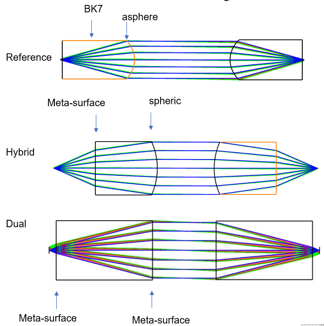
Enter Hybrid Optical Systems - A Perfect Marriage?
In the realm of optics, the integration of meta-surfaces into hybrid optical design has emerged as a revolutionary approach, redefining the possibilities of light manipulation and imaging technologies. The synergy of traditional optical components with meta-surfaces has unlocked novel ways to control light at the nano scale, enabling an unprecedented level of control and customization in optical systems.
The integration of meta-surfaces into hybrid optical designs has not only enriched fundamental research but also stimulated innovation across numerous industries. From telecommunications and medical imaging to augmented reality and autonomous vehicles, the practical applications are vast and diverse.
Nevertheless, challenges remain, such as enhancing the efficiency and bandwidth of meta-surfaces, improving their scalability for mass production, and expanding their capabilities to handle complex optical tasks. As research and development continue, these challenges are gradually being addressed, promising even more exciting breakthroughs in the near future.
The combination of meta-surfaces’ nano scale light manipulation capabilities with conventional optics’ familiarity and robustness has birthed hybrid optical systems that offer unprecedented control, efficiency, and miniaturization. As we continue to explore the potential of hybrid optical design with meta-surfaces, the future holds the promise of even more groundbreaking applications in light manipulation and imaging technologies.
We are eager to take a look with you to check the opportunities of such systems for your optical system. We have an experienced team with the dedication, passion and creativity to get potential new views on existing spec sheets that need better performance, less space, fewer components, etc
Detailed Presentation – Dispersion Engineered Hybrid Meta Surface for highly compact optical systems : accessible here
Dispersion engineering is the technique of tailoring the spectral response of the meta-atoms in a meta-surface to control the wavefront shape and how it changes inside the operating spectrum.Meta-surfaces that rely on wavefront shaping, like meta-lenses but also diffractive lenses have a chromatic focal length shift where the longer wavelengths are focussed closer and shorter wavelengths are focused further away. A unique aspect of meta-surfaces is that by designing the meta-atoms for specific phase dispersion (also called group delay), this chromatic shift can be controlled.
Dispersion engineering has been used to create achromatic meta-lenses or hyper dispersive lenses. Having the capability to tune the chromatic shift of the system within the meta-surface gives the designer a powerful new option that would other wise require multiple components.
The video below explains how dispersion engineered components are designed using the PlanOpSim software. You can find the presentation slideshere.
The video below is part of a workshop presented at the META Conference 07 2022 in Malaga, Spain By Lieven Penninck, CEO of PlanOpSim.com.