Meta-surface designs with high manufacturability in PlanOpSim
General introduction - PDK?
A Process Design Kit (PDK) is a collection of essential components, design rules, models, and data used by integrated circuit (IC) designers to create semiconductor devices, such as microchips and integrated circuits. PDKs are widely used for electronic Integrated Circuits and photonic Integrated Circuits (PIC). Since the end of 2023 PDKs are finally available for metaoptics. Just like in PICs a PDK con-tains the building blocks that are needed to make functional metasurfaces. What’s more PDKs are re-useable, optimized for fabrication and validated before release.
PDKs are specific to a fabrication process and manufacturer. The manufacturer checks and ensures that the building blocks inside the PDK library are compatible with their processing. In this way PDKs serve as a critical bridge between the manufacturing process and the design of semiconductor devices. PDKS will play a similar bridge role in metaoptics.
PDKs as accelerator for the MetaOptics Revolution
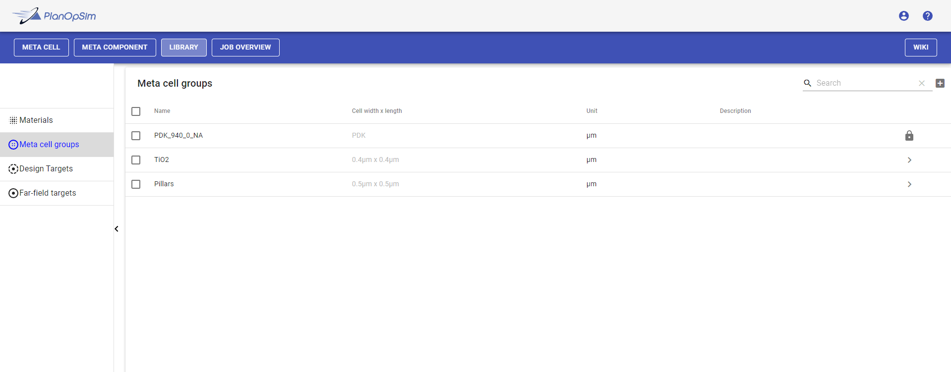
PDK inspection from meta-cell group library.
Picking a PDK group
Select PDK for metasurface design
What are the benefits of a PDK ?
A PDK simplifies and standardizes the work of designers and fabrication labs. These are the main advantages of designing using a PDK:
1. Efficiency: PDKs significantly speed up the design process by providing designers with pre-validated and standardized components. This reduces the time and effort required to create custom semiconductor designs from scratch.
2. Reliability: PDKs ensure that the designs adhere to the foundry’s manufacturing process and design rules, leading to higher reliability and manufacturability of the final product.
3. Consistency: By providing a consistent framework and set of rules, PDKs help maintain design consistency across different design teams and projects.
4. Manufacturability: PDKs are tailored to specific manufacturing processes, which means that designs created using PDKs are more likely to be manufacturable with high yields.
5. Reduced Errors: PDKs help designers avoid common errors, as they include design rules that prevent violations, leading to fewer design iterations. Curious about tolerancing for metaoptics? See our detailed study here.
6. Cost Saving: Faster and more efficient design processes save both time and resources, reducing the overall cost of developing semiconductor devices.
Why are PDKs important to metasurfaces?
Large scale adaptation of any technology is only possible when reliable and high quality production methods are available. PDKs enable such a break-through for metasurfaces.
By using only structures in the PDK library, compliance to the manufacturers design rules is ensured. In other words designers receive scalability and reliability. A downside is there is less design freedom and so some flexibility is sacrificed.
A standardized PDK also avoids a lot of duplicate work in process development, design optimization, and tolerancing. Next to that thanks to PDK via multi-project wafers (MPW), hardware prototypes can be made significantly faster and with processes that are used in mass production.
Fabrication the last domino stone
MetaOptics Fabrication
Fabrication is often thé thing to get fixed No breakthrough without hardware correctly present
If you want to dive deeper into the why? Find a detailed study here.
One of the key questions for the metasurface community is how to fabricate these components both on a laboratory scale and in high volume production. Metasurfaces are a highly active field of research and the fabrication methods are developing rapidly. This article provides an overview of the different approaches being used to fabricate metasurfaces today as well as the advantages and drawbacks that need to be considered for different methods. The choice of which approach is most suitable depends on many parameters: the application, which materials are used and the production facilities that are available.
How to design with a PDK library?
PDKs are accessible in the PlanOpSim software as Meta-cell Group library. Using a PDK library for a metacomponent design, works in the same way as any other Meta-Cell group of your own design. You can see available PDKs in your accounts’ library but editing is locked.
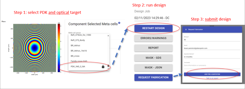
To make a PDK based design:
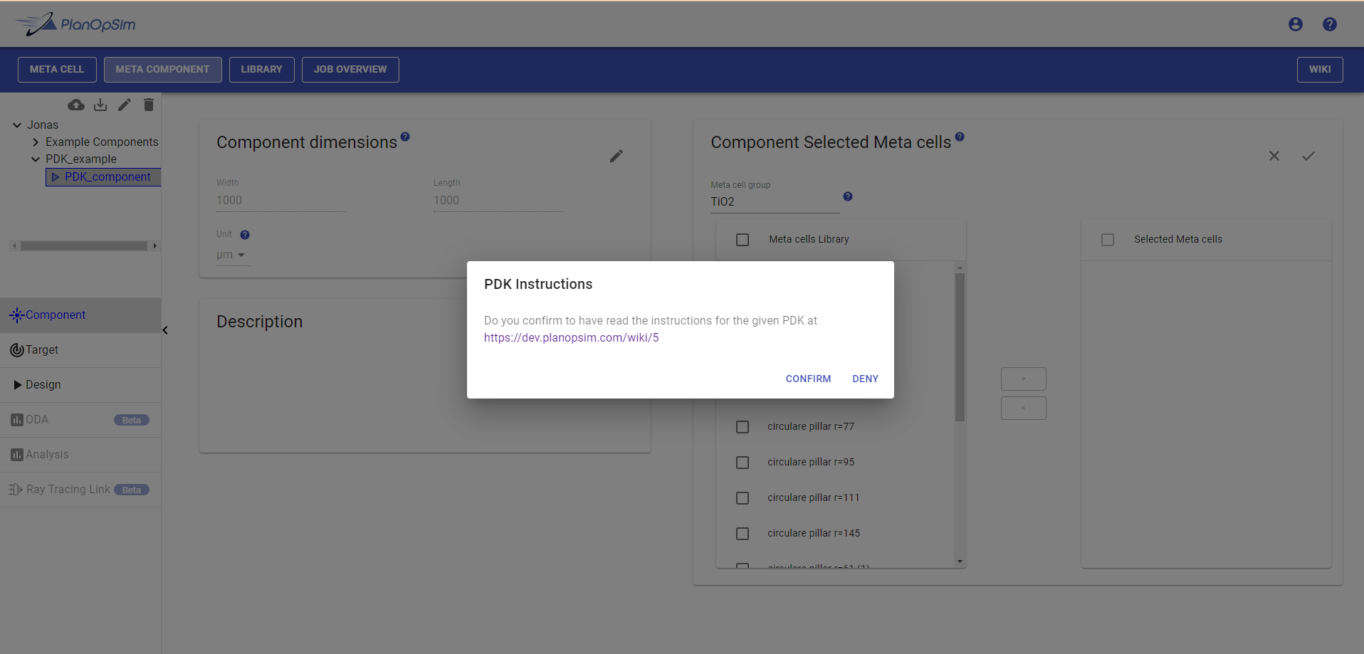
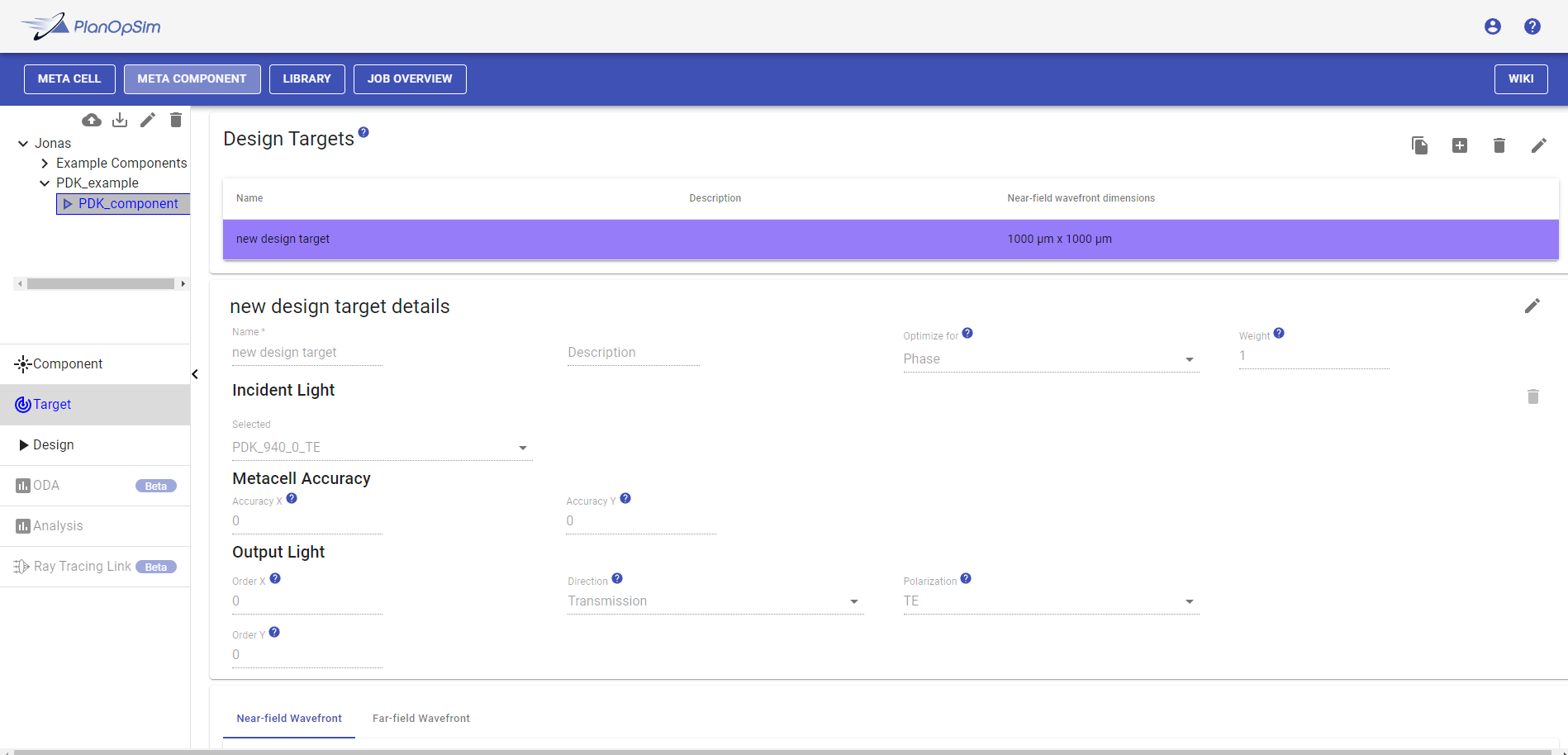
1. Create a meta-component, set the required dimensions and select the PDK of you choice as the “Selected Meta-cell group”. Consult the wiki-page to make sure the PDK you selected is adapted to the spectrum, polarization and field-of-view you are designing for.
2. Set the wavefront targets for different incident conditions (wavelength, polarization, angle) and beam type. The software checks if your design is compatible with the PDK publishers processing geometry, wavelength range, angle of incidence and polarization.
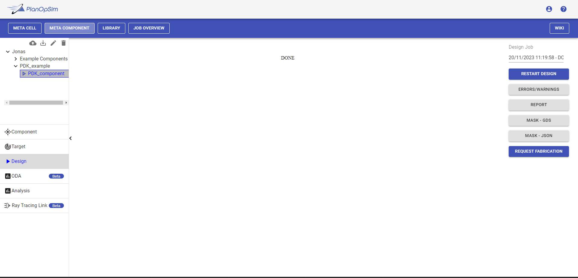
3. Run the design, the software will then optimize the placement of the metaatoms in the PDK.
4. Analyze the components performance in the analysis tab.
5. When the design is ready it can be sent to the manufacturer that provided the PDK to start component orders via MPW. At this point your design will be shared with the manufacturer to estimate costs and timing. Our experts can also guide you through this process and answer any questions you have.
The manufacturers proprietary structures are represented as a black box in the GDS design. In this way sensitive design and manufacturing information is kept confidential. Click here for a video showcasing this into our software or click on the video below.
1. Process Technology Information: This includes details about the manufacturing process, such as the minimum feature size, layer composition, and available materials. It specifies the fundamental building blocks that designers can use.
2. Device Models: PDKs contain models that describe how transistors, diodes, capacitors, and other electronic components behave in the given process. This information is essential for designing circuits that work correctly and efficiently.
3. Design Rules: Design rules are a set of guidelines that designers must follow to ensure that their layouts are manufacturable. They specify minimum distances between features, layer stacking rules, and other restrictions.
4. Extraction Rules: These rules help designers extract electrical properties from the layout and models, which are crucial for simulating and validating the circuit’s performance.
5. Simulation Models: PDKs provide simulation models for various components, enabling designers to simulate and analyze circuit behavior before physical fabrication.
6. Libraries: Libraries include pre-designed components, such as standard cells, memory cells, and analog blocks, that designers can use to assemble their circuits quickly.
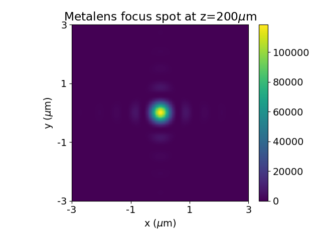
Metalens Example
Fixed Selectable Library
How can you access?
Every customer who has access to our platform, will be able to access this from 01/12/2023.
Every prospect can make use of the 30 day trail to create, generate, analyse and request a quotation for
Fixed Selectable Library
We have boosted it even further with MPW !
Every customer who has access to our platform, will be able to access this from 01/12/2023.
Every prospect can make use of the 30 day trail to create, generate, analyse and request a quotation for