Initial Design and Benchmarking of An InfraRed Meta-Lens
This example contains the design of a meta-lens for infrared applications in the PlanOpSim [2] software
Reading time: 20 minutes
Written for: optical engineers, photonics engineers, researchers, technology scouts.
Extra-relevant if you are interested in: meta-surfaces, infrared optics
Application examples: microscopy objectives, telescope objectives, lightweight optics
IR meta-lens specifications:
Wavelength | 10 µm |
substrate | Germanium n=4 |
lens | Aspherical , f=12 mm |
Clear aperture | 4 mm |
Numerical Aperture | 0.164 |
Metacell | Circular-cylindrical pillars or holes |
Cell size | 2 x2 µm (=λ/n) |
Metasurface size | 4 x 4 mm |
Summary of the Design
· An AR coating is used together with Ge pillars to increase the transmission
· Choose a value for the pillar height where the transmission is maximally close to 1 and simultaneously, the phase shift spans from -180° to +180°. This can impose considerable thicknesses, of the order of approx. λ/2. For a wavelength of 10 micron, this means that we have to work with layer thicknesses of around 5 micron.
· Construct a complete cell-family (critical step in order to obtain a correct near field).
· Impose spherical phase profile for the meta-lens
· Calculate the far field of the aplanatic lens, using the PlanOpSim software tool
In pre-computer times, lens calculations by ray tracing were done by hand, and lens design was a long and tedious job. Hence designers used all their ingenuity and tried to implement smart shortcuts to find the solution with a minimum of rays. With the advent of modern computers, sophisticated search and optimization routines replaced the tedious handwork of the pioneers. The lens assembly can now be optimized in terms of correcting aberrations, by minimizing a target
function which is related to the set of rays launched in the input pupil of the lens. Sophisticated routines exist to calculate the path in parameter space from initial guess to solution, even in a highly dimensional parameter
space.
Designing meta-lenses however relies not on rays but on a full vector wave simulation of the propagating fields. This makes the computations mathematically complicated since we cannot use the concept of “ray” any longer. Moreover, each cell of the meta-lens needs to be positioned individually in order to synthetize the desired phase profile. Hence the number of calculations rises fast in case the lens surface is considerable
Meta-lenses can also be designed at long infrared wavelengths. The major reason for using infrared meta-lenses instead of regular lenses is the cost of the substrate. Infrared materials such as Germanium and Zinc Selenide are costly and the price is proportional to the weight of the component. Meta-lenses minimize the required volumes and hence the cost of the component. To explore the design possibilities of the PlanOpSim software regarding infrared lenses, we investigate how to design an aspherical lens in Germanium for use at 10 micron. We have selected specifications for this lens which are commonly found in commercial lenses. The aim of the paper is to find out if the IR design procedure is different from the established design for he visible spectrum and if we require specific design strategies for IR design.
In this report we opted to analyse a known benchmark lens model, and then evaluate how the PlanOpSim software could be used properly in order to arrive at a good result. The goal was to investigate if designing infrared metasurfaces creates extra challenges for finding a satisfying solution. We did this by benchmarking our results against a recently published paper [1].
Metasurface design contains two main phases. The first is to identify an appropriate meta-atom architecture in order to identify the proper near field wave front of the lens. The required software tool here is the RCWA method implemented in the PlanOpSim MetaCell module. It is of importance to know that this software module is also capable of simulating regular stacks of thin films on a substrate. In this way, a number of design approaches could be applied from classical thin film design. The best example here, is the anti-reflection (AR) coating on Ge. This coating is required, since due to the high refractive index of Ge, an uncoated sample loses 30% of transmission, just by Fresnel losses. So in a subphase of the first phase, we optimized the amplitude transmission of the meta-atoms, by applying a layer of ZnS and varying its thickness. In the second subphase, we optimized the transmitted phase behaviour of the cells.
The second main design phase is to stitch together the different family members, coming from the first main phase, in order to synthesise the desired far field amplitude and phase profile. In this phase, the use of an efficient iterative Fourier Transform algorithm is imperative. For this phase we used the PlanOpSim meta-component Module.
Ultimately, the chosen cell family should cover the [-180° +180°] phase interval, in order to be match the desired near field wavefront.
Specific Design Options
The high refractive index of Ge is responsible for the serious Fresnel losses at input and output faces of a bare Ge substrate at IR wavelengths. A thin AR layer of low-index material is hence classically required to realize a decent transmission. We will follow this rule, and also apply a layer of ZnS in order to control the amplitude of the transmitted wave.
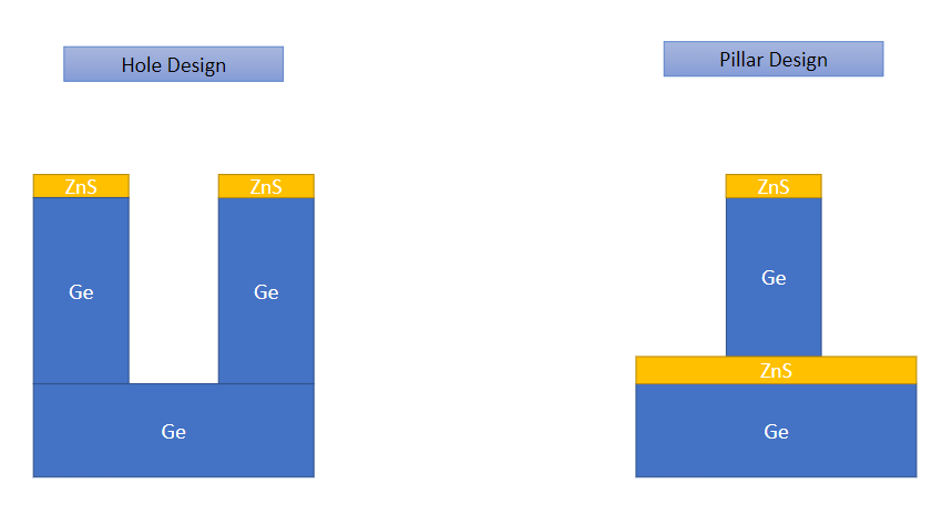
Figure 1: cell geometry: Hole Design & Pillar Design
Next to controlling the amplitude of the near field, we have to consider also the phase profile and how the shape of the metacell is influencing this parameter The cell family should be complete for this purpose. This means that its members can deliver every phase which is required by the phase relation in the phase interval from 0 to 2 pi (1).

Another issue which needs to be addressed is the choice of compatible materials: the extra layers should stick well to Ge and should evaporate while growing in a columnar structure. Finally, we want to master the thickness requirements: these have repercussions onto the fabrication process: longer evaporation times and larger crucibles are required in case of thick layers.
Selected Designs
We have investigated two different architectures of metacells on the Germanium substrate. The first one is made up of cylindrical pillars. The second one consists of circular holes.
To increase the transmission, we provided an AR layer consisting of ZnS. This material is highly compatible with Germanium and is universally used in infrared germanium components.
The thickness of the ZnS layer was first optimized, using the metacell design module as thin film calculator. As starting value, we used a classical quarter wave thickness for this AR layer.
The next figure shows the lay-out of the two selected design options:
The simulations revealed that the hole design delivered a better transmission, and therefore we discarded the pillar design and picked the hole design as the final choice for our metacell design. This is the final configuration of the cell:
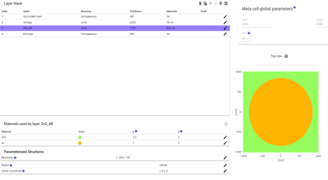
Figure 2 definition of the metacell in PlanOpSim
Then the library
of meta-atoms was formed by selecting a number of values for the hollow pillar
radius, and used to calculate the near field of the lens. Specifically , the
radius was varied between 100 and 900 nm. Here it is of importance to try to optimize
two parameters simultaneously: the transmission and the phase of the wavefront.
The transmission was in fact already optimized through the implementation of
the ZnS film, so that we only had to check if the family could generate every
phase between 0 and 2 pi.
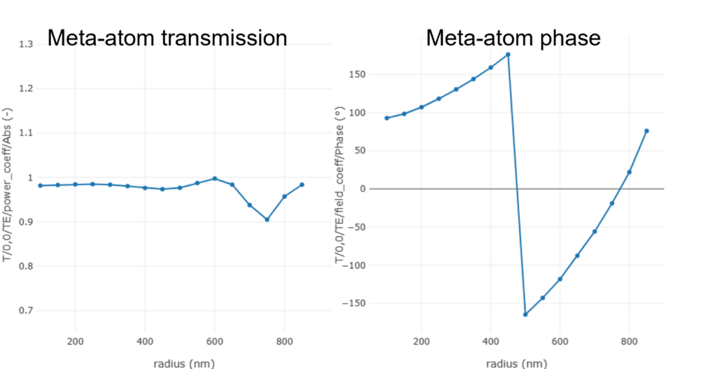
Figure 3 amplitude transmission and phase of the metacell group
The phase variation covers a complete swing of 360 degrees. So we compose a cell library based on these structures. The lens focal distance was 12 mm, the diameter was set to 4 mm (in order to limit the required memory capacity of the computer).
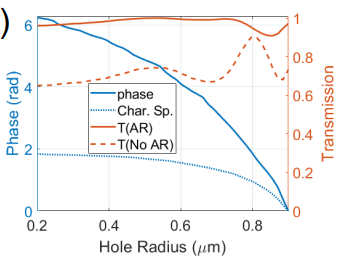
Figure 4 transmitted amplitude and phase of the bench
mark lens
Note that in Fig.(3) the shape of the phase curve for the bench mark lens is convex (increasing with the radius) while the PlanOpSim software delivers in Fig. 3 a concave curve (with an immaterial phase jump); This artifact is due to a difference in convention between the two software tools. In PlanOpSim, a converging wavefront has a positive radius, see Eq.(1) ( decreasing with the radius).
The second part of the design process was carried to with the MetaComponent module of the PlanOpSim software, being the determination of the far field, occurred with good efficiency, Near Field Wave Front Efficiency 0.95, Far Field Wave Front Efficiency 0.67.
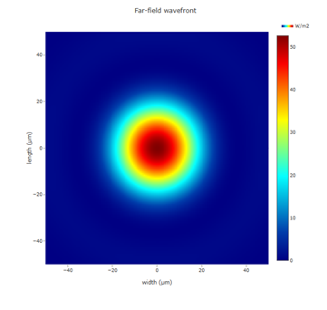
Figure 5 Far field intensity of the simulated lens (25x)
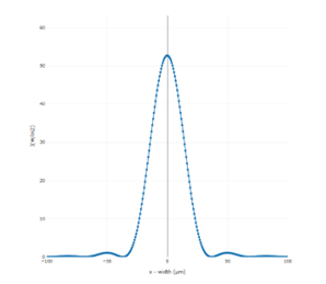
Figure 6
cross section of the far field in
the PlanOpSim software. Note the typical rings around the central Airy spot.
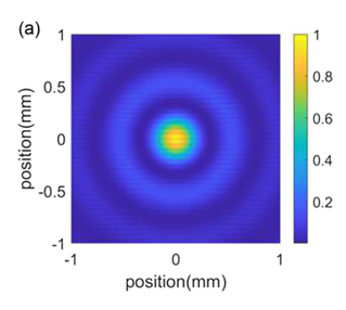
Figure 7 far field intensity of the benchmark lens
The PlanOpSim software also exhibits faint diffraction rings around the central Airy spot, which are barely visible in the colour 3D plot. But due to the colour coding of the graph, it is not well visible in a full colour plot. The rings are clearly visible however in Fig.(6), if we make a cross section of the focal area.
High Energy Use
The PlanOpSim software also provides field calculations inside the MetaCell module. This instrument can be used to our advantage, if the component is meant for use in high energy laser applications. It is known from detailed modelling studies that the interfaces between the thin films on the component are sensitive to laser damage, delamination and ablation. It is not the temperature which is the scaling parameter in this damage mechanism, but the electrical field strength [3]. The laser is capable of reaching the same field strengths as in molecular or atomic bonds in high energy applications.
It is therefore a design rule to prevent high field strengths located at the interfaces. We have looked in detail to the field distribution into a hollow pillar cell of 550 nm radius. As shows fig. 8, there is a field concentration at the Ge/ZnS interface, which would indicate a poor high-energy performance.
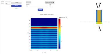
Figure 8 cross section
of a pillar
However, if
we look to a top view of the Poynting vector at the height of the interface, se
Fig. (9) , we see that the energy is concentrated inside the hollow pillar, and
not inside the material. The field intensity is hence concentrated in the air
and not in the Ge or ZnS part of the structure.
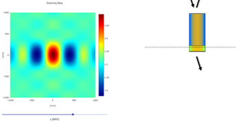
Figure 9 Top view
of the field intensity
We hence
can conclude that the hollow pillar design is capable of handling high energy
pulses and that the risk of damage or delamination is minimized.
Summary of the Design Process
·
An
AR coating is used together with Ge pillars to increase the transmission
·
Choose
a value for the pillar height where the transmission is maximally close to 1
and simultaneously, the phase shift spans from -180° to +180°. This can impose considerable thicknesses, of the order
of approx. λ/2. For a wavelength of 10 micron,
this means that we have to work with layer thicknesses of around 5 micron.
·
Construct
a complete cell-family (critical step in order to obtain a correct near field).
·
Impose
spherical phase profile for the meta-lens
·
Calculate
the far field of the aplanatic lens, using the PlanOpSim software tool
Conclusion
In this design example we successfully design a meta component for the long-wave infrared spectrum. This design example is based on a benchmark design from the literature (A. Sözak, ‘Transmission optimized LWIR meta-lens’) and simulations are done with the PlanOpSim software. The design features a standard lens function in the LWIR spectrum with a strong efficiency improvement based on a meta-cell based anti-reflection (AR) coating. Similar to refractive optics, an AR-coating reduces the reflection losses, though due to the non-uniformity of the fields the AR-coating has to be co-optimized with the meta-cell structure itself. An average 20% improvement can be reached with a single AR layer.
References
[1] H.C. Nalbant, F. Balli, T. Yelboga, A. Eren, A. Sözak, Transmission optimized LWIR meta-lens, Applied Optics, 61, 9946 (2022)
[2] www.planopsim.com/software, more design examples can be found at https://planopsim.com/design-examples-background/
[3] D. Ristau, editor. Laser-induced damage in optical materials. CRC Press 2015
Authors:
Peter.muys@planopsim.com
Lieven.penninck@planopsim.com