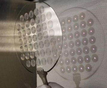
Metalenses and planar optics hold great promise for miniaturizing and simplifying optical systems. They can reduce the weight and volume of bulky assemblies, enable novel functionalities and improve existing lenses and components. Metasurfaces achieve this by covering a surface with sub-wavelength structures that locally manipulate the incident light.
One of the key questions for the metasurface community is how to fabricate these components both on a laboratory scale and in high volume production. Metasurfaces are a highly active field of research and the fabrication methods are developing rapidly. This article provides an overview of the different approaches being used to fabricate metasurfaces today as well as the advantages and drawbacks that need to be considered for different methods. The choice of which approach is most suitable depends on many parameters: the application, which materials are used and the production facilities that are available.
PlanOpSim specializes in simulation software to facilitate the design workflow and communication between design and manufacturing.
How is a metasurface made and why is it difficult?
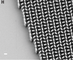
As the name suggests a metasurface is a metamaterial that is applied to a surface (in contrast to bulk metamaterials which are structured in the entire material volume). The structures need to have sub-wavelength sizes for the incident waves to “see” them as a single material. Another way of looking at this is that the unit-cell of an individual structure should be small enough to only diffract the zero-th order (also called a zero-order grating). If the unit-cell woulkd be larger a part of the incident light will be lost due to diffraction into higher diffraction orders.
For example, with an operating wavelength of 1550nm, a cell-width of 1000nm is often used to fulfil the “zero-order” condition. This is the first important aspect in metasurface design, the dimensions of the features to be fabricated become smaller as the wavelength becomes smaller. Metasurfaces designed for the THz regime have millimetre(mm) sized features while for the infrared the feature size shrinks to micrometer and below 100nm for the visible spectrum. When discussing metasurface applications the first order of business should be to specify the wavelength range because that determines which fabrication routes are viable.
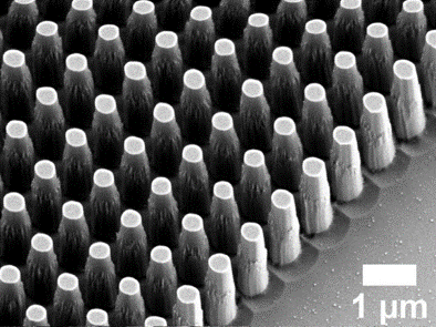
Within the individual cells structures have to be defined to manipulate the light. These different structures are designed to have specific reflective or transmissive behaviour depending on the polarization, wavelength or angle of the incident light. They are what makes the metasurface “work”.
To achieve that behaviour the structures can in principle have any shape. In practice the choice of shapes and structures needs to both achieve the desired functionality and to be manufacturable. The design of structures (using computer aided design tools and electromagnetic simulations) and the fabrication are strongly inter-dependent.
For almost all manufacturing routes the minimum feature size and the aspect ratio (defined as structure height over smallest feature size) are the most important limitations. Where those limits are situated is determined by a complex relation of material choice, maturity of the fabrication process and infrastructure available for the project.
What fabrication technologies are being used for planar optics fabrication?
The fabrication routes for metasurfaces can be divided in three categories
- Lithographical methods
- Pattern transfer methods
- Direct writing methodsLithography
Lithography is by far the most used and most mature fabrication method. There are 2 main steps in the lithographical fabrication of a metasurface:
- Pattern Definition in resist polymer or a hard mask
- Structuring of the functional layer via etching or lift-off
E-beam lithography and photo lithography differ in the way the resist is exposed (the “writing” of a pattern into the resist). This is respectively done by a scanning electron beam or illumination with UV light through a mask.
Photo-lithography is the mass-manufacturing technology applied for chip fabrication. It is capable of high volume production at low cost but the initial tooling effort is high. In photo-lithography an illumination mask has to be made first which is then re-used during many exposures.
E-beam lithography is inherently more suited for R&D. The direct writing via electron beam allows to define patterns with nanometer resolution without having to create any masks. This makes e-beam lithography much more flexible than photolithography but also limits the speed of fabrication. Most R&D work has therefor been done using e-beam lithography.
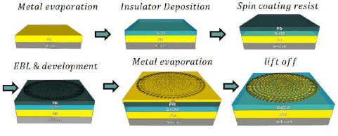
The second key step is the structuring of the active layer via lift-off or etching. The purpose of this step is to transfer the pattern that was defined in the resist (a sacrificial material) to the functional material(s).
Common issues in the structuring step are over- and under-etching leading to non-vertical sidewalls. This causes the structure’s shape to differ from the designed geometry. Ideally the occurrence of over- and under-etching is taken into account and compensated over multiple iterations of the design of nano-structures. In some materials a directional etch procedure can overcome these issues.
Pattern transfer methods
An alternative way to define the patterns is by imprinting a mould into a soft material., like a cure-able polymer. The most often used pattern transfer method is called nano-imprint lithography. As the name suggests, nano-imprint lithography is capable of defining structures on the nanometer scale. As a rule of thumb feature sizes down to 50nm can be achieved .
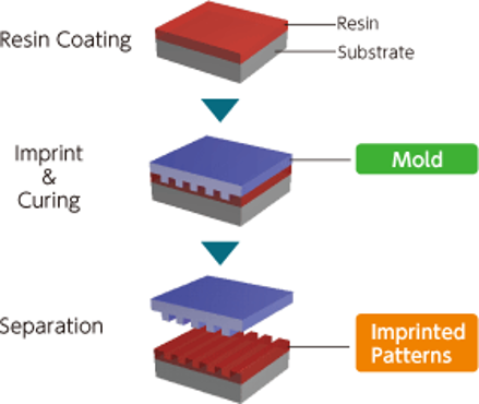
Nano-imprint lithography is an attractive method because it is cost effective and can be applied at high throughput. The most important drawback of this method is that the maximum aspect ratio is lower than what can be achieved by lithography combined reactive ion etching or lift-off method. The master mould can be fabricated by milling, or lithography depoending on the reequired feature size.
Direct writing methods
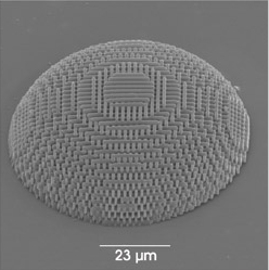
A third approach to metasurface fabrication are the direct writing methods. Among these, two photon polymerization is the most often used. In two photon polymerization a focussed laser beam is used to “write” the sub-wavelength structure directly into a photo-polymerizable material. A non-linear (two photon) polymerization is used to define features smaller than with a conventional (single-photon) polymerization.
An advantage of two-photon polymerization is that it allows to 3D print complicated structures directly into the material. This kind of sub-micron 3D printing has significantly matured in the past decade and commercial tools for this technique have become available on the market. An attractive feature of the technology is also that higher aspect ratios (up to 20 is reported) can be achieved than with etching and lift-off techniques.
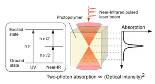
Like e-beam lithography the direct write methods suffer from long fabrication times since each voxel needs to be “written” one after the other. The photopolymer also poses a limitation because polymer materials usually have relatively low refractive indices. The low index is not a fundamental problem but does necessitate higher aspect ratios.
Which manufacturing technique is suitable for my application
To find out which fabrication method is most suitable for a specific project, a series of basic questions needs to be answered.
- What is the target spectral range of the application?
- Which materials can be used?
These parameters will determine the feature size of the metasurface. If the wavelength is large enough and lower refractive indices can be accepted two-photon polymerization and nano-imprint are attractive methods. In many cases there is a trade-off between refractive index and aspect ratio, lower index materials require taller structures. If the high refractive index of dielectric materials is needed either photo- or e-beam lithography is more suitable.
Once the spectrum and list of possible material(s) have been selected it is necessary to find out which nano-structures will give the desired optical properties (for example their reflection and transmission, phase and polarization). This step is carried out using a full wave optical simulation which solves Maxwell equations in detail for the sub-wavelength structure (PlanOpSim offers a dedicated software tool for these calculations).
The result of the nanostructure design is a “family” of nano-structures that will be placed inside the metasurface. The aspect ratio and feature sizes of these structures together with the materials of the structures and substrate will then further limit the available fabrication options.
PlanOpSim specializes in simulation software and design of metasurfaces and can help you in selecting appropriate techniques.
Further reading & Sources
If you wish to explore the topic of metalens fabrication in further depth, these review articles provide a good starting point:
[1] V.-C. Su, C. H. Chu, G. Sun, and D. P. Tsai, “Advances in optical metasurfaces: fabrication and applications [Invited],” Opt. Express, vol. 26, no. 10, p. 13148, 2018.
[2] A. She, S. Zhang, S. Shian, D. R. Clarke, and F. Capasso, “Large Area Metalenses : Design , Characterization , and Mass Manufacturing,” vol. 26221, no. 2014, pp. 26212–26221, 2016.